

This article is taken from a joint issue of the Southeast Asia Chronicle (No. 66Jan.-Feb. 1979) and Pacific Research (Vol. 9 No 5-6 July-Oct. 1978) - "Changing Role of S.E. Asian Women" — about women and women workers
The article 'Women's Place in the Integrated Circuit" by Rachael Grossman offers a documented look at new corporate strategies for social control on the job, and the attempt to orient every facet of employees' lives around the company's plant. It is a first hand report featuring interviews with women in Hong Kong, Malaysia, Indonesia and the Philippines, who talk about the impact of these policies on their lives and about their efforts to resist them.
The following article describes the global assemply line of the electronic corporations
Semiconductors are microscopic electronic circuits which are the latest in a line of technology that began with the invention of the transistor in 1947 and the development of the integrated circuit in the early 1960s. Integrated circuits now bring together up to 100,000 transistors, resistors andother circuitry on a single chip of silicon half the size of a small fingernail. The production of these products is an integrated arxJ very segmented process which includes highly educated scientists in the U.S. and thousands of assembly workers throughout the world.
Semiconductor companies locate their research, development and the initial capital intensive stages of production primarily in the "Silicon Valley" in northern California.
Scientists and engineers design complicated, multi-layered circuit patterns for each semiconductor device, drawing giant versions that range up to 60 inches square. Each design is then photographically reduced until it is virtually invisible to the naked eye.
Assembly workers in California fabricate the initial stages of the semiconductor based on the microscopic negatives. First they "dope" the layers of silicon with various chemical impurities in order to create electrically conductive and nonconductive areas. These positive and negative specks act as transitors, tiny electronic switches that shuttle the electrical circuit about. Other workers then photograph the circuit pattern, etching the pattern into the wafer with acids and solvents. These wafers are then baked in ovens at temperatures over 900 degrees Fahrenheit. For this process, assemblers must insert special gases-arsenic, boron and antimony-into the ovens to alter the electrical characteristics of each device in specified ways. This entire process is repeated for each layer of the pattern, often as many as ten times.
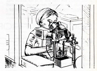
Once the wafers are fabricated, women test each wafer with computerized equipment, sorting them into categories. Because the equipment needed for testing can cost up to $350,000 per unit, this process is generally carried on in or near company headquarters in California.
At this point, wafers are shuttled to Asia. There, Asian women perform the labor-intensive, routine, intermediary assembly operations. When the wafers—2 to 4 inches in diameter—arrive in Asia, workers slice them into up to 500 separate chips. At this point, miles of aisles of assemblers take over to bond these chips to circuit boards. An Assembler peers through a microscope for seven to nine hours a day, bonding each chip with as many as 50 gold wires—each the size of a strand of human hair. Each bonder must work at top speed as individual quotas run as high as 800 chips per worker per day.
Further along the Asian assembly line, other workers bake these chips in 600-1000 degree ovens, sealing each chip inside a plastic or ceramic protective coating. Testers then check the reliability of these components, dipping them in tanks of chemicals and applying electric currents to the components. This step in the process, previously carried out in California, is increasingly being transferred to Asia. Companies either send these components to their other Asian subsidiaries for assembly into simple products such as calculators or they ship the components back to California for the final assembly of products ranging from home computers to military surveillance
systems.
Southeast Asia Resource Center P.O. Box 4000 D Berkeley California 95704 USA Tel: (415) 584-2546
Subscriptions: US$ 8 regular; $ 6 low income; $ 12 institutions; $ 10 foreign surface mail; $ 15 foreign airmail and $ 20 sustaining.
Pacific Studies Center 222B View Street, , Mountain View, California 94041 USA Tel: (415)969-1545